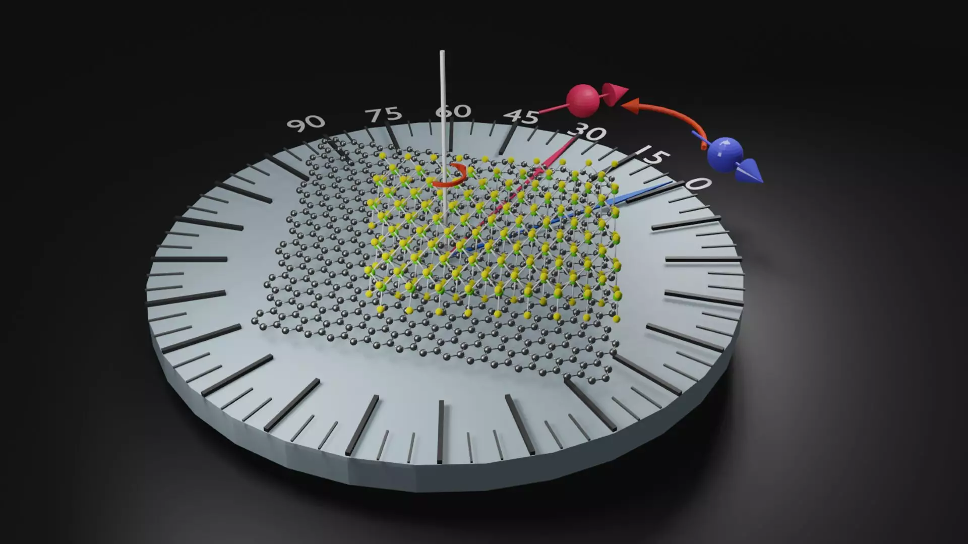
The collaboration between research teams from Charles University of Prague, the CFM center in San Sebastian, and CIC nanoGUNE’s Nanodevices group has led to a groundbreaking discovery in the field of spintronics. This discovery, detailed in a publication in the prestigious journal Nature Materials, introduces a new complex material with revolutionary properties that could shape the future of electronic devices. By stacking two layers of unique two-dimensional materials, namely graphene and tungsten selenide (WSe2), researchers have unveiled remarkable characteristics that have the potential to enhance the efficiency and advancement of electronic devices significantly.
The research focuses on the stacking process of graphene and tungsten selenide layers, emphasizing the influence of minute rotations between the layers on the resulting heterostructure’s properties. Dr. Félix Casanova, the co-leader of the Nanodevices group at nanoGUNE and a prominent figure in the study, highlights the generation of spin current in a specific direction by precisely rotating the two layers. Traditionally, spin transfer occurs in a direction perpendicular to the electric current, posing challenges for spintronics applications. However, the innovative approach adopted in this study demonstrates the elimination of this limitation by utilizing suitable materials and precise layer stacking techniques.
Spin manipulation is a critical aspect of spintronic devices, enabling the storage, processing, and transmission of information using the spin properties of electrons and other particles. The conventional hurdles associated with managing spin currents are surpassed in this study through the strategic alignment and rotation of graphene and tungsten selenide layers. By exploiting the ‘magic’ twist in the stacking process, researchers have unlocked novel spin-related properties that surpass the capabilities of individual materials, paving the way for enhanced spintronics applications.
The implications of this research extend beyond fundamental scientific exploration to practical applications in electronic devices. The integration of magnetic memories into processors, with the aid of the newly discovered material properties, holds the promise of developing more efficient and advanced electronic systems. The emergence of spin-related phenomena through controlled layer stacking introduces a paradigm shift in spintronics, offering unprecedented opportunities for innovation and technological advancements.
The collaborative efforts of research teams have resulted in a significant milestone in the realm of spintronics. The strategic design of complex materials through precise layer stacking techniques has unlocked new potentials that were previously unattainable. As the findings continue to inspire further exploration and experimentation, the future of electronic devices appears brighter and more promising, driven by the innovative discoveries made in this groundbreaking research endeavor.

